
Carving Up the TPU
Leftovers for Jensen or Just Gravy on the AI Trade?

The first words of our August State of the Themes AI section were direct: Long GOOGL.

We elaborated…
OpenAI is compute-constrained. Without their own datacenters or their own chips, they are at significant disadvantage to Google, which not only is an ascendant hyperscaler but also a chip designer that has designed the only mass produced chip competitive with Nvidia’s core offering across many metrics and has optimized their entire research, training and inference pipelines for it [...]
Google has low customer acquisition costs, best-in-class first party data, full vertical integration and TPUs enabling cheaper training [...]
It’s clear that both the technical and market tailwinds favor Google, but the market does not seem to be pricing that in.
While the writing has been on the wall for some time, the market’s perception of Google has dramatically reversed over the past several months – transforming from an AI loser bleeding its search dominance to a stalking horse destined to undercut the most consensus AI winners.
We can see this shift occurred around the time we wrote up Google (or, perhaps, around the time the legal overhang lessened) on this chart from Coatue:
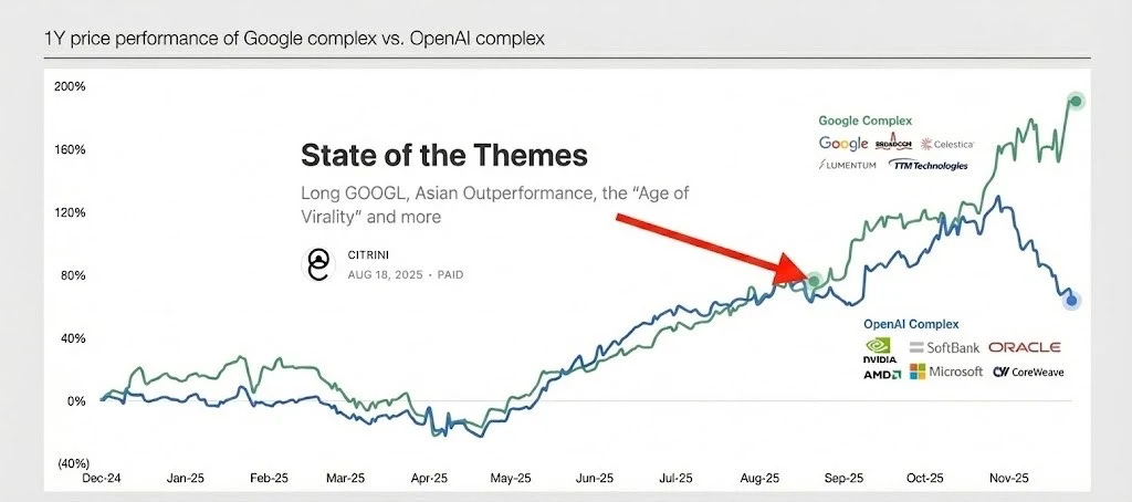
This sentiment has only accelerated in the past week with the release of Gemini 3. Not only is Google now firmly positioned at the cutting edge of frontier models, but it’s doing it on its own terms, or TPUs. It is indeed possible to train a frontier model without NVDA... that is, if you’re an ML-pioneering hyperscaler who has spent the past 10 years developing and optimizing for this custom silicon.
The announcements that both Anthropic and Meta are planning to implement TPU chips raise further questions about NVDA’s dominance. Surprisingly, META reportedly wants TPUs for training, not just inference. None of this information is truly new (see above) but the one-two punch, combined with growing skepticism of OpenAI seems to have culminated in a passing of the public torch.
While we are happy that the market has caught up to the trade – Google remains our largest allocation in our Dynamic AI basket – we are also wary of over-extrapolation, recency bias, and consensus crowding. After all, as Oracle has shown, you can go from a 40% gap up to CDS watching in a matter of weeks.
Is Google’s vertical integration both a cost and structural advantage? Is the CUDA moat shrinking? Are NVIDIA margins at risk?
Perhaps.
But maybe there are two ways to think about this:
Switching costs for architecture/ecosystem is high for AI accelerators. Gemini 3 should be bullish for compute demand as labs locked into NVDA rush to buy more of the next gen chips to compete.
NVDA’s margins are so high that any competitive threat must be aggressively priced in even if it means higher volumes.
In other words, isn’t a breakthrough model broadly bullish?
The market is clearly leaning on the #2, but we could find ourselves tempted to dip back into NVDA if sentiment overshoots reality. Regardless – if a TPU scale-up is on the horizon, who else stands to benefit?
First, we will run through some technical details, then highlight where we think the broader “TPU trade” goes from here.
TPUs for Idiots
At its core, a neural net is just a machine for doing enormous numbers of weighted sums. For myself (an investor, not an AI engineer), I find it useful to reduce neural nets to:
Inputs x Weights = Outputs
Inputs are arranged as a matrix (a batch of tokens, images, whatever). Weights for a layer are another matrix. Take a simple example: handwritten digit recognition. A 28x28 grayscale image is 784 numbers - the “8-detector” neuron holds 784 weights (28x28). For that individual neuron, the core operation is multiplying each pixel by its weight, adding everything up, and then finally comparing the score against other digits.
Once you scale this up to our modern AI/ML models you’re doing trillions of these “matrix multiplication” (abbreviated as matmul) operations – in effect, a bundled batch of all those weighted sums.
Enter: CPUs, GPUs, TPUs.
A CPU is like one very smart and capable worker – good at anything but slow at repetitive jobs. A GPU is like thousands of generalized workers. A TPU is like an automated factory line built specifically for one task, with the machines arranged so the work has almost no back and forth.
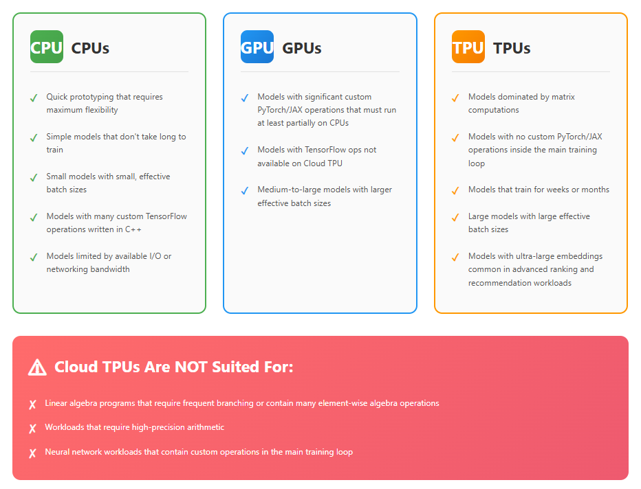
It’s important to recognize that even within the AI/ML space, different functions require different chips. Google itself publishes the following guide for how to choose chips depending on the task at hand.
As we laid out in Interconnects 101, the layman’s understanding of the difference between a CPU and GPU is that a CPU is built with a relatively small number of cores, but with each of those cores capable of executing hundreds of specific instructions over dozens of units. Consumer CPUs generally have up to 16 cores with data center chips up to 128 but even with significantly higher clock speeds, this is no match for the parallelization that GPUs allow.
What we think of as a ‘core’ in a GPU is known as a streaming multiprocessor (SM) in Nvidia-parlence. Rather than focusing all of the core’s resources on routing instructions through specialized units, GPU SMs leverage dozens or hundreds of copies of the same units simultaneously. For example, Nvidia’s Blackwell architecture SMs each have 4 “tensor cores” and 128 “CUDA cores” for a B200 with 192 SMs, that totals 768 and 24,576 physical cores respectively.
Though not comparable on a core-to-core basis, TPUs take this philosophy to the next level and dedicate nearly the entire silicon area to crunching matmuls. They can do this because cores aren’t instructed in the traditional sense, but data is drawn through them more like an assembly line than a laboratory.
The architectural driver behind the TPU is the systolic array. Though reports differ on the size and arrangement of the array across TPU versions, the philosophical departure from GPU SMs is consistent.
The array is made up of MAC cells, short for multiply-accumulate, which Google describes as ALUs (arithmetic logic unit) which is a classic computing building block. The difference is that MAC cells are ALUs that don’t accept instructions, just data. They don’t have to choose between FMA, ADD, SHIFT, or any other of hundreds of possible instructions that a less specialized processor might see – they just multiply and accumulate. This saves on space by eliminating unit-level instruction caches while also essentially eliminating data caches as data flows through the array in a predetermined fashion and saves on power by pushing utilizations to the max.
This is why TPUs can offer very high performance per watt and per dollar on machine learning, but are essentially useless outside that domain. You get extremely high throughput on the kind of linear algebra that defines neural nets which means lower power per operation and a smaller die area for a given level of ML performance. However, this comes at the price of much less flexibility than a GPU.
Google has made Gemini’s per-prompt footprint a PR point, so Gemini likely has a real advantage in energy per text call – helped by TPUs and their own tuning – but there is no transparent or quantified comparison for the training runs. Inference, at least, looks to be much more energy efficient per user interaction on TPUs.
In short, the TPUs are hyper-specialized ML chips that sacrifice flexibility for efficiency. But as AI increasingly moves to the “mass-production” phase, even small efficiency gains can prove very meaningful.
What Does it Mean for NVDA
We’ve been wary of the competitive risks from ASICs to Nvidia for a while (and a TPU is in fact an ASIC). But we’re also wary of headlines that declare Nvidia dead. If our own DeepSeek coverage taught us anything, it’s that the easiest way to move the US stock market (which is a KPI for many financial media outlets) is to target Nvidia.
As we’re indifferent to moving the market and more focused on what happens over the long term, we’re trying to minimize sensationalism.
One key thing to emphasize is that switching from GPUs to TPUs means learning a new language – i.e. switching ML frameworks from PyTorch to JAX. Switching software environments is a significant task – non-trivial, disruptive and expensive. After all, the first TPU was created by Google back in 2015, and the giant has spent the last ten years developing internal workflow, physical infrastructure and model architecture around it. For others, particularly smaller players, the learning curve will be far steeper.
However, Nvidia’s silicon stranglehold and pricing power does provide a material incentive to at least attempt to diversify. Anecdotally, OpenAI has been trying to build an internal JAX equivalent for the last year – newer startups deciding to build initially on JAX rather than PyTorch can result in new “locked-in” users. Moves by Meta and Antrophic demonstrate that major players are indeed seeking silicon diversity.
But the reality is that CUDA and PyTorch are still dominant today and will probably mean that Nvidia will continue to see strong demand in the near term regardless of Google’s plans for TPUs (i.e. whether they sell, rent, or keep it as a walled garden). Keep in mind, despite its use of TPUs, Google is still one of NVDA’s largest customers.
We can certainly understand the market’s sensitivity to any risk that might jeopardize NVDA’s competitive dominance – even if it doesn’t materialize until 27/28. It isn’t surprising that the kneejerk reaction was for NVDA to trade lower. Still, it should be understood as a reaction to the potential of future risks – and future risks to margins, not to volumes. The market is not valuing Nvidia on what happens in 2026, and Nvidia’s margins are (historically speaking) unsustainable over the long term. As seen in the reaction to NVDA’s great earnings last week, the market cares much more about what things look like in five years than what they look like in six months.
Right now, NVDA is still able to deliver volume into a tight market, and overall we view this TPU development as much more positive for GOOGL than it is bearish for NVDA – in fact, we don’t really think this specifically is bearish for NVDA or their supply chain.
Rather it’s probably quite bullish for the supply chain. Both Google and Nvidia are going to be fighting for the exact same CoWoS capacity at TSMC, which will remain the rate limiting factor.
To recap:
Gemini’s success reinvigorates model competition - reinforcing broad demand for compute, which is still dominated by NVDA
CUDA/PyTorch is still a major switching cost, and Google’s success on TPU may not be as easily replicable for third parties
Both supply and infrastructure bottlenecks, not demand, is the key bottleneck today
Will Google Sell TPUs?
Another open question is Google’s TPU distribution strategy:
Do they keep TPUs for themselves as a competitive advantage?
Do they rent out TPUs (which they do already, via GCP)?
Do they become a merchant TPU vendor and alternative to Nvidia?
The first alternative – full in-house proprietary advantage – risks under-monetizing an incredibly valuable asset (remember, NVDA is worth more than GOOGL today) and has already been contradicted by chip sales to Anthropic, Meta, and Fluidstack.
In the second alternative – the “cloud route” – Google is limited by both TSMC capacity and the physical availability of their own data centers. Here, they may maintain ongoing cloud revenue, but are still both committed to and constrained by infrastructure.
However, if Google decides to become a selective merchant vendor (shipping TPUs into neoclouds, sovereigns and selective hyperscaler datacenters i.e. META) they would generate revenue and gain presence without committing to infrastructure. In a world where stocks get hit every six months on capex fears, this might be a good way of hedging. Data center and power capex is very long-duration and hard to unwind. By contrast, selling TPUs is essentially a pure margin game with variable production that can be ratcheted down. This shifts risk and produces optionality, making Google harder to kill.
In a somewhat reflexive way, we think the market’s reaction here is going to force Google to sell TPUs. If they don’t break out TPUs as merchant revenue and data center/power constraints cap GCP capacity growth, then the narrative will become a refusal to monetize the silicon while being subjected to an infrastructure bottleneck they do not control.
Further, if Google does not sell TPUs, they will end up creating space for a new merchant silicon threat in the medium term (think 4-7 years). It would be much better to broadly distribute TPUs and gain the telemetry advantage rather than risk this business going to a competitor (especially a Chinese one).
Back in September, it was reported that Google approached Crusoe, Coreweave (CRWV US) and Fluidstack to give them access to TPUs. Fluidstack, for example, has a deal where it deploys TPUs in a Terawulf (WULF US) leased data center in NYC – with Google providing a $3.2 billion backstop and taking 14% equity. In doing so, they’re using the “franchise” model versus the “merchant” model (you find the power and build the shell, we will drop in our TPUs). Furthermore, this week, we saw headlines about Meta (META US) buying TPUs from Google. Meta has its own silicon (MTIA), but if Google offers TPUs at a better price/performance ratio for serving Llama models, Meta is rational enough to use them.
In short, we believe the decision has largely already been made to begin selling TPUs.
So, what’s the trade?
Below the paywall is our comprehensive list of beneficiaries that sell into the TPU supply chain.